- B2B Industrial Supplier since 1999
- Shipping from our own warehouse in NL !
- Shipping in EU with DPD Traceable
- Reliable SSL & Secure Payments


Compatibility :
U3 Series, T7 Series, U6 Series, UE9 Series
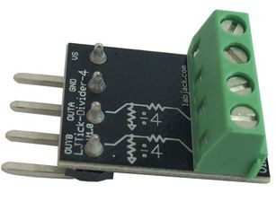
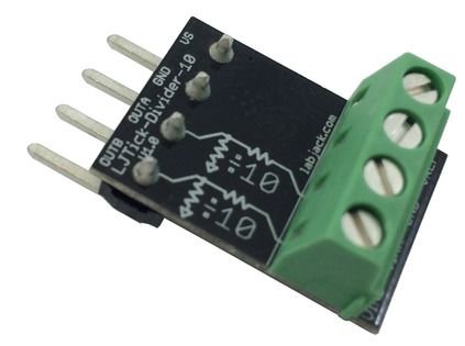
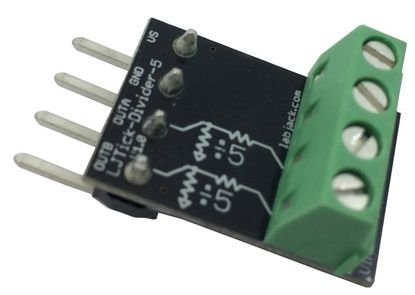
LJTick-Divider
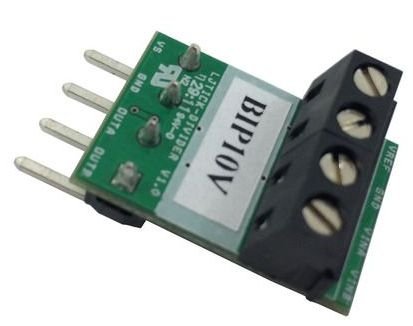
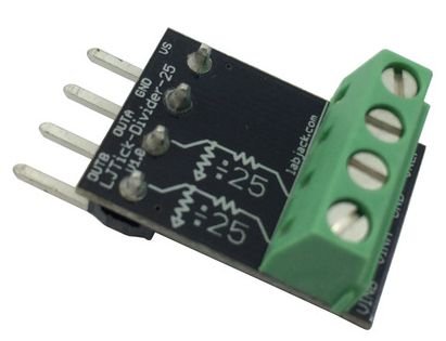
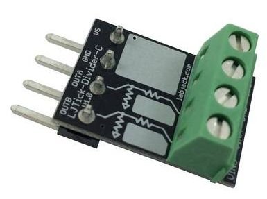
The LJTick-Divider (LJTD) is a signal-conditioning module designed to divide 2 single-ended channels of higher voltage analog signals down to 0-2.5 volt signals. The stock builds are for 0-10 volt inputs (UNI10V) or ±10 volt inputs (BIP10V). The 4-pin design plugs into the standard AIN/AIN/GND/VS screw terminal block found on newer LabJacks such as the U3, U6, and UE9. The use of large resistors and a precision op-amp buffer provide an input impedance of 1 MΩ. By adding or replacing resistors, many other configurations are possible.
Prior to December 2007, all shipped LJTick-Dividers were the UNI10V configuration and were not specifically labeled. Starting December 2007, all shipped LJTick-Dividers have a label specifiying UNI10V, BIP10V, or other.
VINA/VINB: These screw terminals are for the 2 single-ended channels of input analog voltages. With the factory default configurations (UNI10V or BIP10V), the input to either of these terminals is typically 0-10 or ±10 volts, and produces 0-2.5 volts on the respective OUT pin.
GND: Same as LabJack ground. VINA/VINB must be referred to this ground.
VREF: A 2.5 volt reference voltage output. Internally this reference is used for level shifting, but very little current is used, leaving substantial current available to the user if a very accurate 2.5 volt reference is needed.
U6: The LJTD is used with the +/-10 or +/-1 volt range on the U6. With the +/-10 volt range the full 0-3.5 volt output of the LJTD can be measured, but only 3.5/20 = 17.5% of the U6 input range is used. With the +/-1 volt range, the 0 and 1 volt output columns above apply, and 50% of the U6 input range is used.
UE9: The LJTD is used withe the 0-2.5 or 0-5 volt range on the UE9. The 0 and 2.5 volt output columns above use 100% of the 0-2.5 volt UE9 input range, or the 0 and 3.5 volt columns use 70% of the 0-5 volt UE9 input range.
(1) The maximum input voltage to the buffer amplifier is VS-1.5, so for proper operation with signals up to 2.5 volts, VS must be greater than 4.0 volts.
(2) The input impedance and bias current is dominated by the input resistors not the buffer amplifier. The input bias current of the internal buffer amplifier is less than ±200 pA across the voltage range, which is an important number as far as sizing the input resistors to not create excessive offset.
